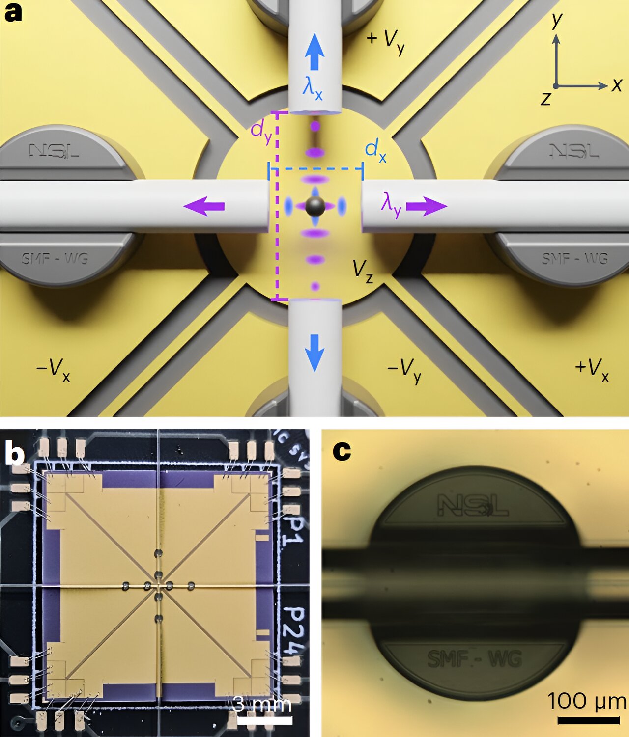
The team’s on-chip levitation platform. a, The top optical layer consists of two orthogonal pairs of split single-mode optical fibers. One of the pairs (along y) creates a standing wave at λy = 1,550 nm, while the second pair (along x) creates a standing wave at λx = 1,064 nm. The distances between the fibers are dx = 80 μm and dy = 160 μm. A particle (black) is trapped at the intersection of both standing waves. The light scattered by the particle in the fibers, shown by the arrows, is used for displacement detection. The four fibers are positioned above a set of planar electrodes used to apply active feedback cooling to the charged particle via electrical forces: right and left electrodes for x feedback, top and bottom electrodes for y feedback, and center electrode for z feedback. b, Image of the levitation chip showing the planar electrodes, four optical fibers, fiber mounts near the center, and wire bonds from the chip to the PCB at the corners. c, Optical fiber positioned in a mechanical mount fabricated via two-photon polymerization used to align and hold the fibers in place. Credit:Nature Nanotechnology (2024). DOI: 10.1038/s41565-024-01677-3
The levitation of microscopic objects in vacuum and the control of their motion while floating was first demonstrated a few decades ago. Since then, several research groups have been working on new approaches to control floating objects in vacuum with larger degrees of freedom.
While most experiments performed to date have relied on optical techniques, some teams have recently begun using hybrid experimental platforms that combine concepts rooted in atomic physics. These hybrid platforms allow for greater control over the motion of levitating objects, unlocking new possibilities such as force and torque sensing or precision acceleration.
Researchers from ETH Zurich recently demonstrated the high-vacuum levitation of a silica nanoparticle on a hybrid photonic-electric chip. Their proposed experimental platform, outlined in a paper published in Nature Nanotechnologywas shown to enable robust levitation, precise position sensing, and dynamic control of the nanoparticle in vacuum.
“Due to the isolation from the environment and the precise control over mesoscopic objects, levitation in a vacuum has emerged as a versatile technique that has already been useful in various scientific fields, from force measurement and thermodynamics to materials science and chemistry,” Bruno Melo, Marc T. Cuairan and their colleagues wrote in their paper.
“It also offers great opportunities for advancing the study of quantum mechanics in the still unexplored macroscopic domain.”
Despite recent advances in vacuum levitation and particle motion control, most previously introduced experimental methods rely on complex strategies and/or bulky equipment. This severely limits their real-world applications, making them impractical for the development of new technologies.
Some researchers have therefore attempted to miniaturize vacuum levitation platforms using electrostatic and optical traps. However, the levitation achieved with most of their proposed approaches was not robust enough to be applied to constrained devices, such as cryostats and wearable devices.
Melo, Cuairan and co-workers introduced a novel hybrid photonic-electric platform that enables robust levitation, position sensing and dynamic control of a nanoparticle on a chip. Unlike other platforms, their proposed method does not require bulky lenses and optical equipment.
“We demonstrate levitation and motion control in high vacuum of a silica nanoparticle on the surface of a hybrid optical-electrostatic chip,” Melo, Cuairan and their colleagues wrote. “By combining fiber-based optical trapping and sensitive position sensing with cold damping by planar electrodes, we cool the particle motion down to a few hundred phonons.”
In initial tests, the team’s proposed on-chip vacuum levitation and motion control platform achieved remarkable results, with signal-to-noise ratios and optical displacement sensing capabilities comparable to other approaches that rely on bulky optical equipment. When they combined their platform with planar electrodes for active feedback cooling, the researchers were also able to cool the silica nanoparticle and reduce its motion in 3D
The new approach to on-chip vacuum levitation and motion control introduced by this team at ETH Zurich may soon open up new opportunities for quantum research and technology development. In their next studies, Melo, Cuairan and their colleagues plan to continue improving their platform, for example by using refractive microlenses to further improve detection sensitivity and integrating more advanced optical elements (e.g., fiber cavities).
“We expect our fully integrated platform to be the starting point for on-chip devices that combine integrated photonics and nanophotonics with precisely designed electrical potentials, improving control over particle motion toward complex state preparation and readout,” Melo, Cuairan and their colleagues wrote.
More information:
Bruno Melo et al, Vacuum levitation and motion control on chip, Nature Nanotechnology (2024). DOI: 10.1038/s41565-024-01677-3
© 2024 Science X Network
Quote: The demonstration of vacuum levitation and motion control on an optical-electrostatic chip (2024, July 2) Retrieved July 2, 2024, from https://phys.org/news/2024-07-vacuum-levitation-motion-optical-electrostatic.html
This document is subject to copyright. Except for fair dealing for private study or research, no part may be reproduced without written permission. The contents are supplied for information purposes only.